Your Tech Story

Semiconductor

ASM International

ASM International: The Biggest contributors in the Growth of Semiconductor Technology

The semiconductor chips or we simply call them the ICs, have transformed the world of information technology. The founding of the ICs has opened doors for many who wanted to try their hands on a new career through innovation. ASM is one such name that came into being during the time when the semiconductor industry started to pave its way. And today, the names ASM and semiconductor technology go hand-in-hand. The company started as a sales agent in semiconductor fabrication technology, and now, ASM is known as the pioneer of new semiconductor technologies like Photolithography, Epitaxy, Ion implantation, and Atomic Layer Deposition (ALD).

ASM International

ASM has been functioning since 1968, the time when semiconductor technology was at its beginning too. The company has been working as a manufacturer of semiconductor wafer processing equipment for the fabrication of semiconductor devices.  The working of ASM includes designing, manufacturing, sales, and service of the semiconductor wafers. ASM International shines as one of the leaders in the industry and serves in various fields, including communications, entertainment, energy, transport, and medicine.
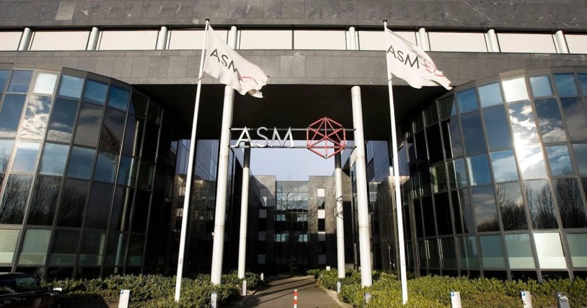
ASM International
Image Source: telegraaf.nl

The Origin of the Company

Arthur Del Prado founded AMS International as Advanced Semiconductor Materials in 1964 in Bilthoven, the Netherlands. He founded the company behind his house in a small shed, where he developed one of the first products of the company. In the very beginning, Advanced Semiconductor Materials was a sales office for semiconductor fabrication technology. In 1968, it registered as a private limited company.

In the next ten years, in 1970, ASM started its own designing and manufacturing unit for chemical vapor deposition equipment. With the hard work of Prado, ASM acquired a semiconductor molds manufacturing company Fico Toolings in 1974. The company also established its first international office in Hong Kong in 1975, which is known as ASM Pacific Technology today. In 1976, ASM had another office opened in Phoenix, Arizona.

In May 1981, ASM had its first IPO, and it was listed on Nasdaq. Del Prado believed in innovation and started to invest in new technologies like lithography, ion implantation, epitaxy, and wire bonding. This helped the company to grow at an even faster pace. The company then, in 1988, divested ASML Holding N.V. and ASM Ion Implant and ASM Fico to Berliner Electro Holding in 1993.

Different branches of ASM started to focus on diverse technologies to achieve faster results. The ASM Europe was working on the vertical low-pressure chemical vapor deposition furnaces, ASM Japan focused on plasma-enhanced chemical vapor deposition, and ASM America targetted the single wafer epitaxy.

At the beginning of the 2000s, the company was working on the 300-mm wafer technology and atomic layer deposition and introduced the latter in 2007. ASM was among the top ten global companies in the first Institute of Electrical and Electronics Engineers (IEEE) Spectrum study, 2006. The 45nm node and the Pulsar ALD tool from ASM became the first system to be used in the high-volume manufacturing of devices using a new hafnium-based high-k dielectric material. In 2009, the company headquarters was shifted from Bilthoven to Almere, the Netherlands. Currently, the company is working on device geometries of 10nm and below.

The Founder: Arthur del Prado

Arthur del Prado is the name of the legend who has a great contribution to the field of the semiconductor industry. He was born on 17 November 1931 in Dutch East Indies. During the Second World War, he got separated from his family and was locked in a Japanese camp as a teenager. But fortunately, he met his family again after the war was over.

ASM International Founder
Image Source: asm.com

Del Prado joined the University of Twente and studied chemistry, and later, went to the University of Amsterdam to pursue a degree in economics. He also went for further studies at Harvard Business School in 1954. He came back to the Netherlands in 1958, and in 1964, he founded ASM International. Del Prado served ASM as the Chief Executive Officer until 2008 and as the Chairman until 2016. He passed away in September 2016 at the age of 85.

ASM Today

ASM International is known to be the biggest contributor to the growth of the semiconductor industry. The company is currently having its various branches in 16 different countries, and over 2337 employees are working for it. ASM is the major producer of the products in the Atomic Layer Deposition, Epitaxy, Chemical Vapor Deposition categories. Benjamin Loh is the current CEO of ASM International.

Apple

Apple Faces Stern Chip Challenge in Replacing Qualcomm Modems

Apple Inc is one of the world’s largest technology companies with investments in various sectors and fields. Recently, the company made a foray into the world of semiconductors and chipsets. The switch has helped make Apple a powerhouse within the semiconductor industry in the past decade or so. The move impacted several major manufacturers who earlier used to supply chips to the American tech-giant. However, the iPhone maker will soon face their sternest test in the coming years. The biggest and toughest challenge that Apple will face will be Qualcomm. In this article, we will take a look at what Apple needs to do to replace Qualcomm’s cellular modems with its unique design.

Can Apple Succeed?

On Friday, Qualcomm slumped to its steepest decline since mid-June when it fell by over 7% to $144.28. Bloomberg was the first to report in June that Apple was entering the modem industry by kicking off development on its unique design. However, this reaction severely undermines the challenges that Apple will have to face to make it in this industry. According to analysts and experts, Apple will b confronted by the primary task of replacing Qualcomm in the coming years. Many also questioned whether the California-based tech giant had bitten off more than what it could chew. With doubts swirling around the industry, Apple will have to come back strong with a design that is both unique and highly functional.

Apple

Questions Raised

A representative of Raymond James, Chris Caso mentioned that the most significant questions that experts have are when and if Apple will be successful. Many experts believe that there are no assurances that Apple will be highly successful in developing a high-end and cutting-edge modem. However, modems are one of the most vital elements that make up an iPhone. It is the part that is responsible for connecting the phone to various cellular networks. Without this device, people could no longer browse the internet, message their friends over the internet, or make phone calls. Hence, ensuring that this component works smoothly and seamlessly is vital to ensuring the mobile in itself is successful. However, designing and crafting a modem requires specialized engineering and critical and broad industry knowledge and know-how. Both of these might take significant time to acquire, which Apple does not possess.

Other options and issues

Meanwhile, wireless carriers work differently as the networks built to support them use distinct radio frequencies. But, in that case, the equipment required to capture these waves are also very different and must conform to various stringent local government rules. As a result, modems have to integrate seamlessly with different technologies and fit into older systems as well with ease. The ever-growing need for cellular data and technical prowess makes this divide and the need for complexity even more considerable. Hence, field testing will be an integral part of the research and development process. 

What Qualcomm Does Right

To facilitate such testing, Qualcomm has labs that work towards replicating the varying environments that mobile phones will face. These labs accurately predict and run scenarios that phones will experience around the world. Additionally, engineers spent decades working with various carriers to fine-tune their technology and integrate it seamlessly over the years. It is this experience and knowledge that has helped Qualcomm rule the semiconductor and modem industry all this time. It is also precisely these qualities that served as a barrier to other tech companies that wished to work their way into the lucrative semiconductor industry.

Expert Opinion

Analysts at Bernstein Research mentioned that while Apple has a history of immaculate expertise in semiconductor design. However, even with all that expertise, modems are very challenging to design and get right. The company took around five to ten years to come up with a sustainable and viable processor for the personal computer system. Experts believe that modems pose an even more significant challenge than PC processors, making this a difficult journey for the American giant.

Also, Qualcomm enjoys another vital advantage when compared to Apple. It regularly collaborates with players in the wireless industry and helps in the development of cellular standards. As a result, most of their chips are the first to market when it comes to functionality and features. This has been one of the things that have helped Qualcomm maintain its lead over its competitors.

However, it is foolish to write Apple off since it has in the past taken on influential industry players and won. The company started designing PC processors to displace Intel from being used in Macs. Since 2010, Apple has been using its own processors in the iPhone and iPad. The company has also been successful in developing wireless and power-management chips for the Apple Watch. While the challenge might be harder this time around, users will have to wait and see if it can meet this stern challenge.

Advantest

Advantest- The firm that turned helpful in shaping the future of Japan’s nascent semiconductor industry.

Semiconductors are available on earth in more than enough quantity. However, these are the core component used in a variety of electronic devices. Like smartphones, PCs, electrical household appliances. As well as constitute the parts of automobiles and many other devices. These all devices, in fact, are indispensable to the lives of people. Thus the semiconductors used in such devices must be high in quality, and performance. Many firms are working in this field, and Advantest is one of the names dominating the field. In the semiconductor industry, technology updates alter every single day. While Advantest has always been delivering the product and solutions as per this changing technology.

It is well-known for bestowing to remarkable efficiency in production in the electronics industry. As well, secure and easier the lives of people through its innovative products.

About Advantest

It is a well-known semiconductor firm based in Japan. Manufactures semiconductor products, component test system products, and mechatronics-related products. It is headquartered in Tokyo in Japan. The firm also sells the used electronics components and products through exhibitions. Also, leased the products for commercial use. Additionally, the firm is active in research and development, measuring, and testing technologies.

Network of Advantest

The firm offers it’s services and products to foundries, semiconductor firms, and other firms in the manufacturing industry. It has built a strong network in Japan. As well as covers the other Asian regions, Europe, America, and other parts of the continents.

The backstory of Advantest

Back in 1954, Ikuo Takeda builds the foundation of Advantest as Takeda Riken Industries. Sooner or later, the firm shifted to Oyaguchi-Cho in Itabashi Ward, later on shifting again in Tokyo’s Nerima Ward. In 1957, Advantest release the first product for current measurement. It was Micro Ammeter. One more milestone of Advantest, that time Takeda Riken is the first-ever electronic counter made in Japan.

Advantest
Image Source: digitimes.com

The TR-124B counter helped in exploring the business for the firm and gave it fame as the digital counter company. As well, marked the beginning of innovative products in the companies history. Thereafter, Advantest released many electronics components that were made in Japan for the first time. Such as vibrating capacitance ultra-low-current electrometer, digital voltmeter, etc. The firm touched the new level when it introduced the TR-3189 105 MHz electronic counter, the highest-performance product in the world. Soon this product popular all over the world; in 1962, selected as one of the Nikkan Kogyo Shimbun’s “Top 10 New Products”.

Services and products

To verify the quality, reliability, and performance of the semiconductors that will be used in electronic components, Advantest has Automated Testing Equipment/ATE. With this electrical test, the complex and defects in semiconductors can be detected with great accuracy. It also enabled another method for semiconductor testing i.e. using peripheral devices. Advantest has also been active in Nanotechnology Business, Field services, SLT business, and many other related businesses.

Apart from that, the firm also conducts the sale of use semiconductors, commercial mechatronic products, component test systems. As well, it is active in the device leasing business.

Exploring the business

Starting from its establishment, Advantest used cut edge technology. It developed products that reflect the innovative nature of the firm. In 1980, it released the first tester made in Japan. Thereafter, it launched a memory system having a capacity of 20MHz.

During the 1980s, Advantest’s T-3300 series remarked as one of the Nikkan Kogyo Shimbun’s “Top 10 New Products”. Moreover, the firm produced an intelligent spectrum analyzer of series TR-4172. Because of its multifunction features, it became popular among communications equipment manufacturers. To explore the business furthermore, Advantest acquired Astronics Corporation in 2019. It was working in the field of semiconductor system-level test business. As well as it captured Essai, Inc in 2020, so that it can enable high-precision test solutions than earlier.

Recognition and Awards

Advantest has been selected for FTSE Blossom Japan Index and FTSE4Good Index. The first index measures the performance in environmental practices, and the second one is related to CSR. It is also honored as a 5-Star Company. Also, marked its name in 10 BEST List in VLSIresearch Customer Satisfaction Survey. Not for the first time but for the 31st Consecutive Year.

Yoshiaki Yoshida- CEO

He is serving as CEO at Advantest since 2017. Yoshiaki has been working with the firm for a long time. In fact, he joined the company in 1999.

AMD

AMD – The evolution of semiconductor firm from designing simple Shift register to high tech processors

The semiconductor industry is one of the inherently risky industries. Because we know that technology evolves every year, and people also demand products that use cut edge technology. But the product development cycle generally takes three to five years, so companies need to stay one step ahead of the customer’s demand. It means, the firms need to develop such products in advance that customers will demand a few years later. Thus, if any semiconductor firm doesn’t follow the update then it will be out of competition, surely.

In such a scenario, very few old firms succeed to keep their dominance in the semiconductor industry. Advanced Micro Devices i.e. AMD is one of such names that still have a high reputation and has acquired a large market globally. Since 1969, the firm has gone through lots of evolution as well as up-downs but succeeds to meet the exceptions of every generation.

What is AMD?

A USA based multinational semiconductor firm AMD is well-known all over the world. It is headquartered in Santa Clara in California. The firm is recognized for its computer processors and the development of other technologies for business as well as personal consumers. Mainly the firm has manufacturing units of microprocessors, motherboard chipsets, graphics processors, and embedded processors. These are used for PCs, servers, workstations, and embedded system applications.

How it is formed?

To see the history of AMD’s establishment we have to look back to the year 1969. Yes, it is that old and still stands out than other Rivals. Meanwhile, in 1969, the former executives of Fairchild semiconductor established Advanced Micro Devices to develops their own products. They were almost seven colleagues including Jerry Sanders III, John Carey, Ed Turney, Sven Simonsen, Jack Gifford, and the other three members.

Soon after a year of establishment, the firm released the first product. It was a 4-bit MSI shift register of series Am9300. Also, it launched the logic counter of series Am2501, which was commercially successful. As well, it was the fastest multiplier available at that time. Thereafter, AMD developed many other products including RAM chips, processors, etc.

Products Of AMD

Since 1969, AMD acquired large business as well as consumer market due to its promising products. US Department of Energy also favors AMD’s chips for its project of the supercomputer. As well, the firm is a powering exascale class supercomputer at the Lawrence Livermore National Laboratory. Moreover, the Ryzen processor is a well-known product of AMD. Recently, the firm released the third generation of this product. Another processor called Epyc is a milestone of Advanced Micro Devices, designed for data centers. Apart from processors, firm design CPU, APU, RAM, Graphics products, etc. Athlon, Opteron, Radeon, Radeon Instinct are some of the products of AMD.

Strategy

Standing out in the competition in the semiconductor industry is not a cakewalk. When there are tough competitors like Intel, it gets more difficult. Despite all challenges, AMD stands strong in the industry since it’s the foundation. For this, credit goes to the policymakers and founders. The firm adopted a unique strategy and focus on areas of development of high-performance processors, computing architecture, and gaming graphics chips. While stayed away from entering technology related to mobile phone development, basically the areas outside its core Competencies.

Some of the key founders of AMD

AMD Founders
Jerry Sanders, Jack Gifford, John Carey, Larry Stenger

Walter Jeremiah Sanders III

He is an American businessman and one of the core founding members of AMD. As well, he served as the CEO of the firm for a long time. Before that, Jerry worked at Fairchild semiconductor, a firm that design the first IC.

Edwin James Turney

He shares great contributions in the establishment of AMD i.e. Advanced Micro Devices. Before that, he also worked at Fairchild Semiconductor. At AMD, he served as a vice president of sales and administration for a long time.

Other Founders

The Fairchild Semiconductor’s former employees Jack Gifford, Larry Stenger, John Carey, Frank Botte,  Sven Simonsen, Jim Giles also helped in the AMD Foundation.

Later success

Lisa Su is presently serving as the CEO of AMD since 2014. Under her policy, AMD achieved great success and stability in the commercial market. Though the firm business is affected due to the US-China trade war as well as disruptions due to the Coronavirus pandemic, the firm’s shares are increased by more than 1,300%. Currently, AMD is focusing on the global data center market. While other high-tech companies focusing on next-generation technologies such as 5G, IoT, AI, etc. Last year, AMD stock was the best performing stock in the S&P 500. As well, it is in growing about 150% during this year.

LOGO

St Microelectronics – A European Semiconductor Conglomerate

The usage and importance of semiconductors have increased in the modern era. To suffice the need for efficient telecommunication, semiconductors are of utmost importance. From making an integrated circuit to transistors and microcontrollers, everything falls under the domain of electronics. The demand for electronics engineers and semiconductor companies is rising exponentially with every passing day.

Major semiconductor companies around the world have either emerged from the US (Broadcom) or Asia (Samsung). Japan and China have also proved their excellence in this part. Seeing this Europe finally stepped out and harnessed its potential.

In 1987, STMicroelectronics was established and in 1957 the parent companies of ST were established. The parent companies of ST are SGS Microelettronica and Thomson-CSF Semiconductor. The company is currently based in Geneva, Switzerland.

The parent companies

With America, Korea, and Japan making a significant presence in the global marketplace, Europe was lagging a bit in this field. The Italian and the French government ran SGS Microelettronica and Thomson-CSF Semiconductor respectively before merging. And, they decided to merge the two companies to create something huge and worthy that can compete in the current industrial competition.

SGS was established in 1957 in Olivetti for producing semiconductors and related products. The company didn’t expand because the manufacturing unit was developed only for the local area. In the 1960s it made an agreement with Fairchild Semiconductors and the company started growing. But, very soon it reached saturation and was still insignificant compared to the other companies in the market.

Thomson-CSF was born back in 1879 by Elihu Thomson and Edwin Houston. It was known as a major electronics and defense contractor in France. The company merged with General Electric in 1892 and since then multiple companies merged with it. In the next century, few divisions of this company were sold and the existing parts were divided before privatization.

Formation of STMicroelectronics

The merging took place in 1987. Previously, the name of the new Italian-French conglomerate was SGS-THOMSON which was changed to ST in May 1998. The company changed its fate once the production started. By 2014, the company was ranked 14th on the top semiconductor’s company list.

By the end of 2013, the company made a sale worth $850 million and the annual revenue summed up to $8 billion. In 2014, the company became the 9th largest semiconductor company worldwide in terms of revenue. By this time, ST not only went international but established a market in ten different countries including manufacturing units and research centers. Around 45,000 employees were hired and were in full shape to beat the competitors.

The Success

The company soon filed for an IPO and the first one was completed on 4th December 1994. In 2002, the company started a partnership with Motorola and TSMC. By 2005, ST’s only competitors were Toshiba, Intel, Samsung, and Texas Instruments. It became the largest semiconductor company in Europe famous for making semiconductor chips.

In 2007, ST and Intel started a joint venture and merged Intel Flash Memory activities. In April 2008, ST and NXP started a new partnership concerning mobile activities. The major shareholder was ST owning 80% of the company. Next year welcomed another joint venture of ST-NXP Wireless with Ericsson Mobile Platforms.

ST contributes a very considerable amount in R&D. The main R&D centers of ST are in Geneva, Tours, Milan, and Catania.

Current Status of STMicroelectronics

By 2018, ST hired 46,000 employees among which more than 7,000 worked in the R&D centers. The annual revenue has summed up to $9.66 billion. ST has expanded to thirty-five different countries with 80 marketing offices.

Apart from the main headquarters in Geneva, ST has other headquarters too. The company has established its US headquarters in Texas followed by other branches in Amsterdam, Tokyo, Singapore, and Shanghai. Three headquarters in Asia concludes a rich business in this region.

Towards a better world

With the increasing crisis in our planet for every existing non-renewable resource, ST is more inclined towards producing smart solutions. Sustainability is a key feature of ST and throughout this journey, ST has maintained strict sustainability strategies. ST is a signatory of the United Nations Global Compact for the last nineteen years. The company actively participates in any kind of challenge concerning environmental protection and finds a solution to it.

Jensen Huang : The CEO & Co-founder of Nvidia

An American entrepreneur and a businessman, Jensen Huang is the CEO and co-founder of the graphics-processor company Nvidia. Huang is an all-rounder, who as a child was placed third in junior doubles at the U.S Open and at the same time, was deeply in love with his books. He is a fan of tattoos and his love for cars as well as speed, encouraged him to buy a Ferrari 430, a Ferrari 599 and a Swedish Koenigsegg CCX. Huang is never afraid of failures and believes that it is ‘Okay to Fail’, to achieve your goals.

Early Life

Jensen Huang was born on 17 February 1963, in Tainan City, Taiwan. After some time, his family moved to Oneida, Kentucky, and then to Oregon. His family, along with his elder brother, sent him to live with their relatives, in the United States, when he was just 10 years old. There, the two joined the Baptist School, a school for troubled students. After a few years, both of them were back in Oregon, to reunite with their parents. Huang completed his high school education from the Aloha High School, outside Portland.

In 1984, Huang entered the Oregon State University, where he received a bachelor’s degree in electrical engineering. He further joined Stanford University, to complete a master’s degree in the same, in 1992.

Founding Nvidia

After completing his education, Huang started working at LSI Logic as the Director of the company. He then, joined Advanced Micro Devices, Inc., as the microprocessor designer.

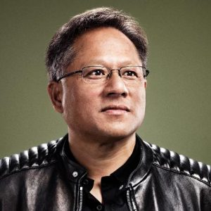
jen-hsun-huang
Image Source: idolnetworth.com

Huang knew that graphics is the future of computers and gaming will be the most revenue generating field in the future. In April 1993, along with his partners, Curtis Priem and Chris Malachowsky, Huang co-founded Nvidia, a software and semiconductor maker company, with a capital of $40,000.

Huang was appointed as the CEO of the company, Curtis Priem as the Chief Technical Officer and Chris as the Senior Vice President for Engineering and Operations. Chris worked at the same position for ten long years, and in 2003, he took retirement from his post.

Nvidia deals mainly in four markets including gaming, professional visualization, data centres and auto. The company has also started working in the field of artificial intelligence.

The company received $20 million of venture capital funding from Sequoia Capital and others. In 2018, the company recorded a 40.6% increase in the revenue of the company, with the earnings of US$3.047 billion.

Personal Life

Huang is married to Lori Huang, who was once his Lab partner in College. The couple has two children with their marriage.

Huang is also into Philanthropy and donated US$30 million to build the Jen-Hsun Huang School of Engineering Center to his alma mater Stanford University.

Ernst & Young named him the Entrepreneur of the Year in High Technology, in 1999. In 2003, he was presented with the Dr Morris Chang Exemplary Leadership Award. In 2009, he received an honorary doctorate from Oregon State University. Huang was named among the world’s top 50 influencers, in the in the inaugural EDGE 50, in 2018.