Chinese Chip Gear Imports Reach All-Time High of $26 Billion in 2024

I am a law graduate from NLU Lucknow. I have a flair for creative writing and hence in my free time work as a freelance content writer.
I am a law graduate from NLU Lucknow. I have a flair for creative writing and hence in my free time work as a freelance content writer.

I am a law graduate from NLU Lucknow. I have a flair for creative writing and hence in my free time work as a freelance content writer.
I am a law graduate from NLU Lucknow. I have a flair for creative writing and hence in my free time work as a freelance content writer.
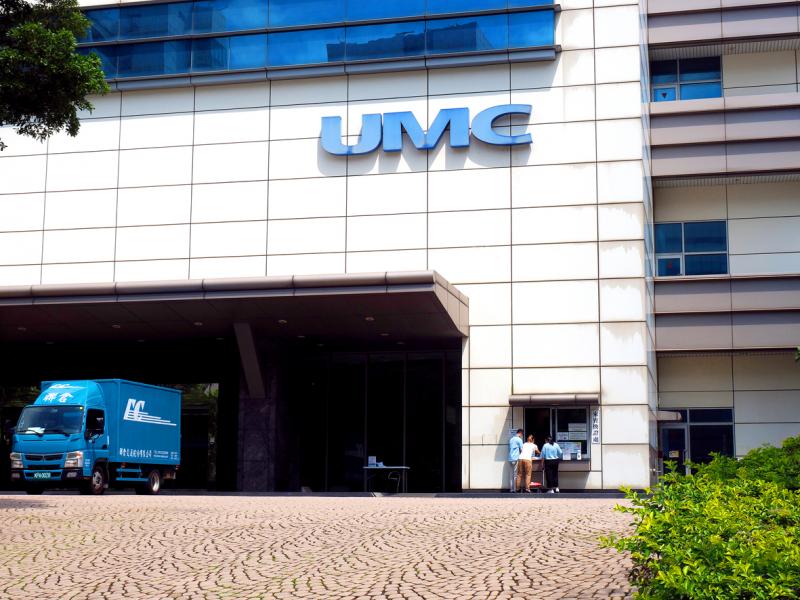
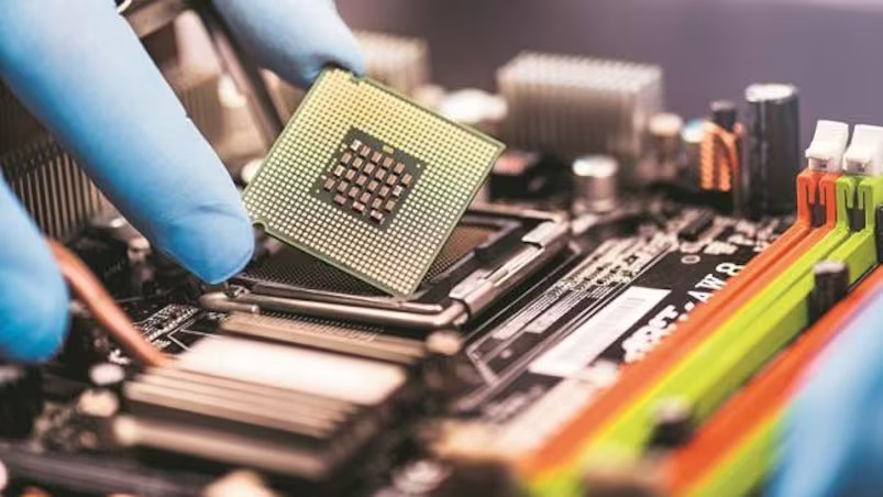
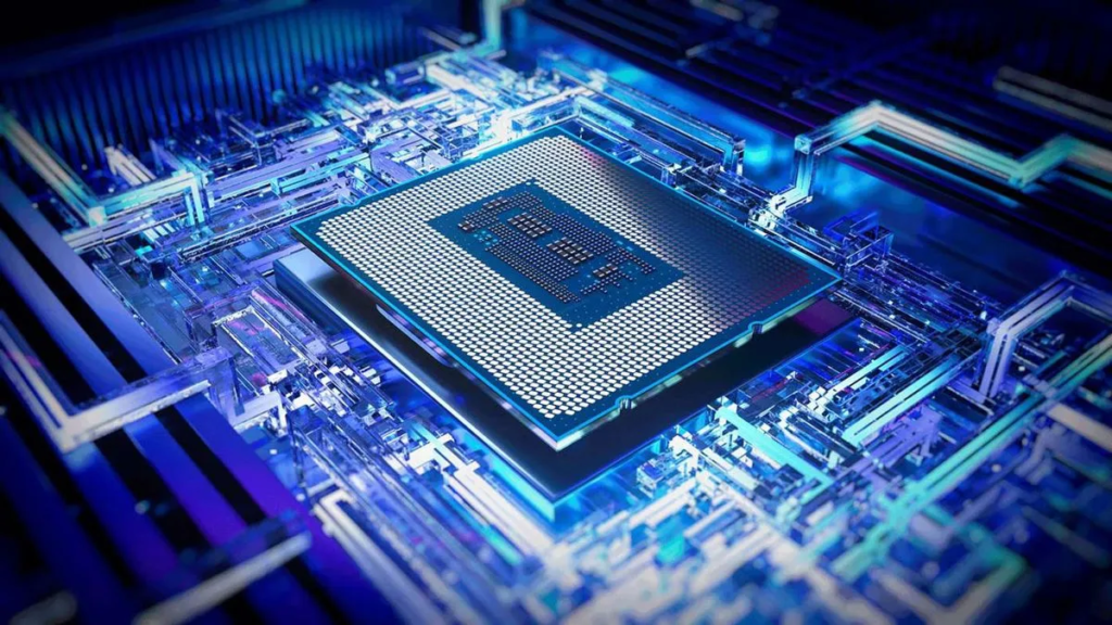
United Microelectronics Corporation is a chipmaker based in Taiwan with around a $10 billion market capitalization. It sells CMOS wafers, memory chips, and high-voltage integrated circuits, among other things. UMC has offices in Taiwan, Japan, South Korea, China, Singapore, the United States, and Europe, with over 17,000 employees worldwide.
About
United Microelectronics Corporation
The
silicon foundry business was where United Microelectronics
Corporation (UMC) established its niche. UMC is a leading silicon
foundry, or contract semiconductor maker, trailing only archival
Taiwan Semiconductor Manufacturing. Design, engineering,
manufacturing, packing, sorting, and testing are among the company’s
production services. It supplies
complementary metal-oxide-semiconductor logic wafers, mixed-signal
wafers, radiofrequency complementary metal-oxide-semiconductor
wafers, embedded memory products, high voltage integrated circuits,
and complementary metal-oxide-semiconductor image sensors through its
semiconductor foundry. UMC has offices in Taiwan, Japan, Korea,
China, Europe, the United States, and Singapore, and it continues to
expand capacity and invest in sophisticated manufacturing technology.
Taiwan is the company’s largest market, accounting for 33% of net
sales. Singapore (24 percent), the United States (12 percent), and
China are the other key markets (9 percent ).
UMC
is aggressively developing internationally. The corporation invested
$48 million in a subsidiary of Fujitsu Semiconductor, which has a
12-inch wafer manufacturing facility in Japan. In Xiamen, UMC has
formed a joint venture with the city government of Xiamen and the
state-owned Fujian Electronics and Information Group to establish a
semiconductor fabrication plant. Starting in 2015, UMC will invest
$1.35 billion in the initiative over five years. In January 2015, the
company bought a 33 percent share in Xiamen-based chipmaker United
Semiconductor as part of the plan. Taiwan’s first semiconductor
company, UMC, was formed in 1980. Since 2012, Yen Po-wen, who joined
UMC in 1986, has served as CEO.
Manufacturing
Diversification
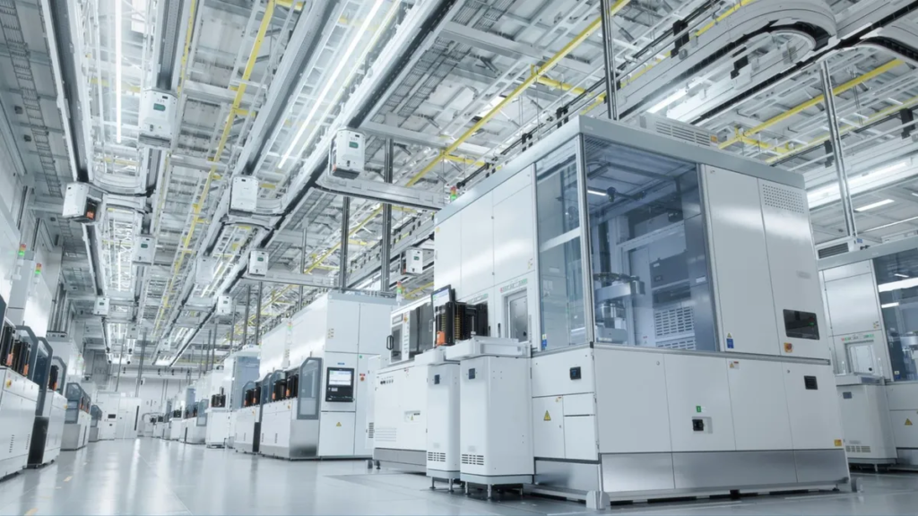
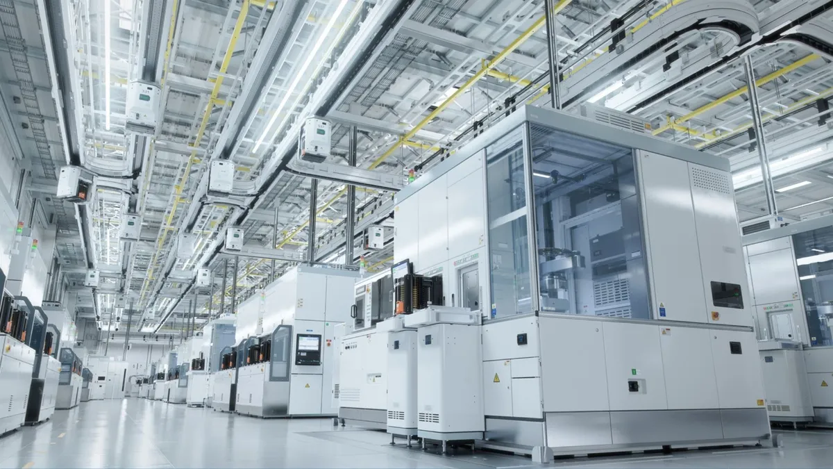
With
numerous modern 300mm fabs in operation, UMC is a foundry production
leader. Since 2002, Fab 12A in Tainan, Taiwan, has been producing
client products in volume and is currently producing 14 and 28nm
products. Phases 1&2, 3&4, and 5&6 make up the
multi-phase complex, which is essentially three independent fabs. The
entire monthly production capacity of Fab 12A is currently above
87,000 wafers. Fab 12i, UMC’s second 300mm fab, is located in Pasir
Ris Wafer Park in Singapore. With a monthly capacity of 50,000
wafers, this second-generation 300mm plant is also in volume
production. United Semi, UMC’s third 300mm fab in Xiamen, China,
began volume production in Q4 2016. When fully equipped, United
Semi’s overall design capacity is 50,000 wafers per month. In October
of this year, UMC bought USJC in Japan. This 300mm fab in Mie
Prefecture has a monthly capacity of 33,000 wafers for logic and
specialty processes down to 40nm. UMC provides reliable and
diversified manufacturing with leading production efficiency, thanks
to its seven 200mm fabs and one 150mm specialized fab.
John
Hsuan and Robert Tsao
From
1979 to 1981, Mr. Tsao was appointed Vice Chairman of the Electronics
Research & Service Organization (ERSO), where he played an
important role. He was a driving force behind the establishment of
the Industrial Technology Research Institute (ITRI), where he oversaw
the development of Taiwan’s first integrated circuit manufacturing
line, which later became the foundation for United Microelectronics
Corporation (UMC), a semiconductor contract manufacturer that
produced chips based on the designs of its customers.
John
Hsuan, who is soft-spoken and aloof at times, has been a driving
force behind UMC’s recent metamorphosis from a small Taiwanese chip
producer to a major IC wafer foundry. UMC was one of the first
foundries to implement a 0.25-micron process, is a pioneer in
0.18-micron technology, and aims to ship products with copper
interconnects early next year. UMC is the world’s second-largest
pure-play foundry, behind Taiwan Semiconductor Manufacturing Co.
Ltd., with sales expected to increase from $1.3 billion in 1998 to
$1.75 billion this year.

I am a second-year student pursuing Liberal Arts from Nmims. I am a painter, I love reading and have a great interest in cooking. I am also a trained kickboxer. I’ve always had a passion for writing and hence in my free time, I work as a freelance writer.

Continuing with the collaborations with Arm, a British semiconductor design company, now Nvidia is again working together with the company to support the processors built by the former. Nvidia announced the news at the International Supercomputing Conference (ISC) going on in Frankfurt, Germany, saying that the partnership will be able to build supercomputers which will “exascale” on performance.
According to Nvidia, the two companies are working towards developing the energy-efficient supercomputers that will be carrying out at least a quintillion (a billion) floating point, i.e. Flops, computations per second. Noticeably, one flop is equal to the multiplication of two 15-digit numbers.
Nvidia’s founder and CEO Jensen Huang, while announcing the news at the event, said, “As traditional compute scaling has ended, the world’s supercomputers have become power constrained. Our support for Arm, which designs the world’s most energy-efficient CPU architecture, is a giant step forward that builds on initiatives Nvidia is driving to provide the HPC industry with a more power-efficient future”.
The company will be extending its support for Arm with its high-performance computing and AI-focused software by 2020. The other services that the company will be offering Arm, includes software development kits, profilers, CUDA-X libraries, PGI compilers with OpenACC support, and graphics-accelerated frameworks, etc.
The partnership between the two companies will help Arm to expand its business and build trust among the investors, as no computer architecture from the company will be without the support of Nvidia. Though it is not the first time that the two are working together, previously, the two had joined hands for Nvidia’s AGX platform that incorporated Arm-based chips and also Nvidia’s Deep Learning Accelerator (NVIDIA).
On the other hand, with this partnership, Nvidia will be getting access to the most energy-efficient chip designs, specially built for mobile devices. According to Nvidia, the energy saving products are the next big thing that is going to be the most important in the coming future.

Yashica is a Software Engineer turned Content Writer, who loves to write on social causes and expertise in writing technical stuff. She loves to watch movies and explore new places. She believes that you need to live once before you die. So experimenting with her life and career choices, she is trying to live her life to the fullest.