Your Tech Story

Sandhya Gupta

I am a law graduate from NLU Lucknow. I have a flair for creative writing and hence in my free time work as a freelance content writer.

The Success Story of Google's Eric Schmidt

The Success Story of Google’s Eric Schmidt

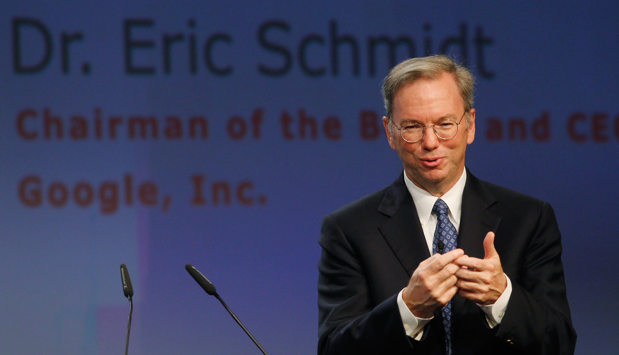
Eric Schmidt was born on April 27, 1955, in Washington, D.C. He grew up in Blacksburg, Virginia, where his father was a professor of international economics at Virginia Tech. Schmidt’s early exposure to academia laid the groundwork for his future pursuits. He attended Yorktown High School in Arlington, Virginia, and went on to earn a bachelor’s degree in electrical engineering from Princeton University in 1976. Schmidt’s academic journey didn’t stop there; he later received a master’s degree and a Ph.D. in computer science from the University of California, Berkeley.

Early Career
The Success Story of Google's Eric Schmidt

Image Source: cnbc.com

Schmidt’s professional career began at Bell Labs, where he worked on network management software. His expertise in computer science and engineering quickly became evident, leading him to various roles in prominent tech companies. He joined Xerox’s Palo Alto Research Center (PARC) and later moved to Sun Microsystems in 1983, where he played a pivotal role in developing the Java programming language. His time at Sun Microsystems marked the beginning of his rise in the tech industry.

Rise to Prominence at Novell

In 1997, Schmidt took on the role of CEO at Novell, a software and services company specializing in network operating systems. His tenure at Novell was challenging, as he sought to revitalize the company amid stiff competition and market changes. Although his efforts were met with mixed results, Schmidt gained valuable experience in corporate leadership and strategic management, setting the stage for his next significant career move.

Transformative Leadership at Google

In 2001, Schmidt’s career took a transformative turn when he joined Google as CEO. Co-founders Larry Page and Sergey Brin recognized his experience and leadership qualities, appointing him to lead the company through its rapid growth phase. Schmidt’s tenure at Google was marked by his focus on innovation, organizational efficiency, and strategic acquisitions. Under his leadership, Google expanded its product offerings beyond search, launching services like Google Maps, Gmail, and Google Chrome.

Schmidt’s approach to management, often described as a “triumvirate” leadership style with Page and Brin, fostered a culture of creativity and collaboration. He played a crucial role in Google’s initial public offering (IPO) in 2004, which solidified the company’s financial foundation and market presence.

Executive Chairman and Legacy

In 2011, Schmidt transitioned from CEO to Executive Chairman of Google, allowing him to focus on broader strategic initiatives and external partnerships. During this period, he was instrumental in guiding the company’s ventures into artificial intelligence, cloud computing, and autonomous vehicles. Schmidt’s influence extended beyond Google, as he became a prominent advocate for technology policy and innovation on a global scale.

Schmidt stepped down as Executive Chairman in 2018 but continued to serve as a technical advisor to Alphabet Inc., Google’s parent company. His legacy at Google is defined by his visionary leadership, commitment to technological advancement, and ability to navigate the complexities of a rapidly evolving industry.

Eric Schmidt’s biography is a testament to the impact that visionary leadership can have on the tech industry. From his early days at Bell Labs to his transformative role at Google, Schmidt’s career is marked by innovation, strategic foresight, and a dedication to advancing technology for the betterment of society. His journey serves as an inspiration to aspiring leaders and technologists worldwide.

The Success Story of BMW's Stefan Quandt

The Success Story of BMW’s Stefan Quandt

Stefan Quandt, a key figure in the automotive industry, is best known for his significant stake in BMW. His journey from inheriting wealth to becoming a strategic and influential leader in the business world is a remarkable story of maintaining and expanding a legacy.

Early Life and Inheritance

The Success Story of BMW's Stefan Quandt

Image Source: press.bmwgroup.com

Born on May 9, 1966, in Bad Homburg, Germany, Stefan Quandt is the son of Herbert Quandt and Johanna Quandt. The Quandt family has been deeply intertwined with the BMW brand for decades. Herbert Quandt, Stefan’s father, played a pivotal role in rescuing BMW from bankruptcy in the 1950s, laying the groundwork for what would become a global automotive powerhouse. After Herbert’s passing, Stefan and his sister, Susanne Klatten, inherited significant stakes in the company.

Education and Early Career

Stefan Quandt pursued his education in engineering, earning a degree from the Karlsruhe Institute of Technology. His technical background provided him with a solid foundation to understand and contribute to the automotive industry. Before fully immersing himself in BMW, Stefan gained valuable experience working at Datacard Group in Minneapolis and at Boston Consulting Group, where he honed his skills in business strategy and management.

Leadership at BMW

Stefan Quandt officially joined BMW’s supervisory board in 1997. His involvement marked the beginning of a new era for the company. While maintaining a low profile, he has been instrumental in driving BMW’s innovation and sustainability efforts. Under his guidance, BMW has embraced electric mobility, autonomous driving technologies, and sustainable manufacturing practices. His leadership style is characterized by a long-term vision and a commitment to preserving the company’s legacy while steering it towards future growth.

Diversification and Investments

Apart from his pivotal role at BMW, Stefan Quandt has diversified his investments across various industries. He holds stakes in companies like Logwin AG, a logistics firm, and shares in Solarwatt, a solar energy company. These investments reflect his interest in sustainable technologies and future-oriented businesses. By diversifying his portfolio, Quandt has ensured a robust financial foundation that supports his ventures and philanthropic activities.

Philanthropy and Personal Life

Stefan Quandt is also known for his philanthropic endeavors. Through the Herbert Quandt Foundation, he supports numerous social and cultural initiatives, including educational programs and scientific research. Despite his immense wealth, Quandt leads a relatively private life. He resides in Bad Homburg, away from the public eye, and is known for his modesty and discretion.

Legacy and Future Prospects

Stefan Quandt’s success story is a testament to his strategic vision, commitment to innovation, and ability to uphold his family’s legacy. His leadership at BMW and diversified investments have not only expanded his wealth but also contributed significantly to the automotive industry and beyond. As the automotive sector continues to evolve, Quandt’s influence and vision will undoubtedly play a crucial role in shaping its future.

In summary, Stefan Quandt’s journey from inheritance to strategic leadership exemplifies how visionary thinking and a commitment to innovation can drive success across generations.

Amazon Plans to Build High-Security Data Center in Australia

Amazon Plans to Build High-Security Data Center in Australia

In a significant move to bolster Australia’s cyber defense capabilities, Amazon.com Inc. has announced a partnership with the Australian government to build a state-of-the-art cloud data system. This initiative is set to handle top-secret information and enhance the nation’s security infrastructure. Deputy Prime Minister Richard Marles revealed the collaboration with Amazon Web Services (AWS), the cloud computing arm of Amazon, at a press conference in Canberra on Thursday morning.

A Major Investment in National Security

Amazon Plans to Build High-Security Data Center in Australia

Image Source: rnz.co.nz

The Australian government has committed to investing at least A$2 billion ($1.3 billion) over the next decade into this ambitious project. While the exact locations of the data centers and the specific nature of the information they will house remain undisclosed, Marles emphasized the critical role these facilities will play in strengthening Australia’s defense capabilities.

“This cutting-edge technology will enhance Defence’s resilience,” said Marles, who also serves as the defense minister. He highlighted that the new system would not only improve the Australian Defence Force’s war-fighting capacity but also strengthen interoperability with key international partners, including the United States. The project is expected to create up to 2,000 jobs for Australians, contributing significantly to the nation’s economy and technological advancement.

Strengthening International Cyber Cooperation

The announcement of this partnership comes as part of a broader trend of countries investing in high-security data infrastructure. In 2021, AWS secured a NZ$7.5 billion ($5.3 billion) deal to build similar centers in New Zealand, and there were reports in the same year that the UK’s intelligence services had signed agreements to utilize cloud services for their top-secret data.

Under the new agreement, Amazon will construct three purpose-built facilities across Australia. These centers will primarily store top-secret information from the country’s defense and intelligence agencies, enhancing the security and operational capabilities of these critical sectors. This strategic collaboration is expected to deepen security cooperation between Australia and the United States, reinforcing the alliances that underpin global security frameworks.

In conclusion, the partnership between Amazon and the Australian government marks a significant step forward in fortifying the nation’s cyber defense infrastructure. As the world increasingly relies on digital information and cloud services, such investments are crucial for maintaining national security and ensuring resilience against emerging threats. The new high-security data centers will not only provide robust support for Australia’s defense operations but also signify a strong commitment to international cooperation in the realm of cyber security.

Ex-Banker Behind Chipmaker Renesas Chases $100 Billion Value

Chipmaker Renesas Chases $100 Billion Value Under Ex-Banker’s Leadership

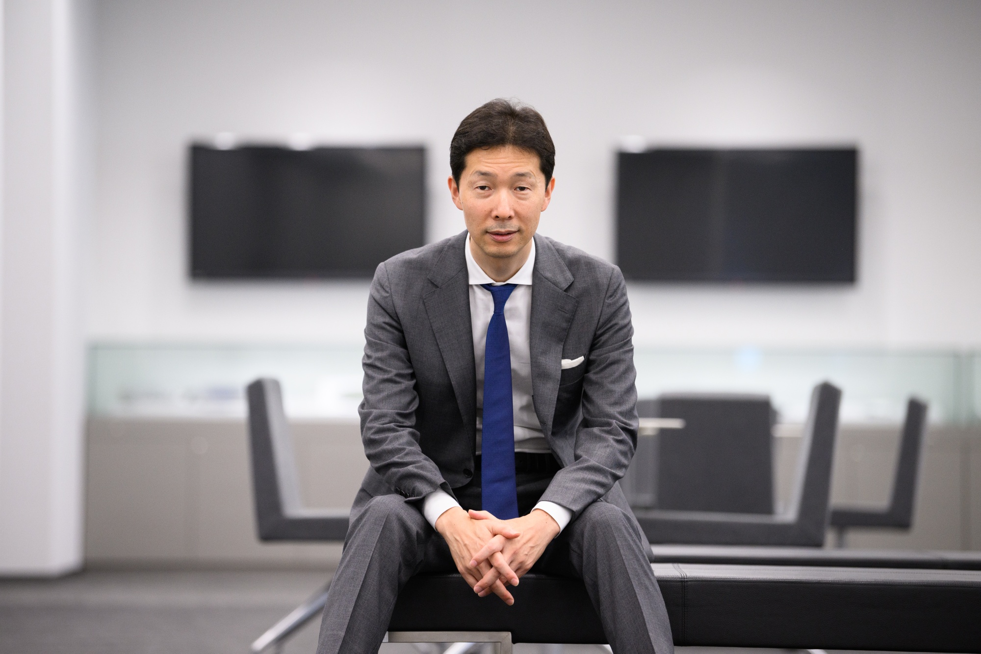
A decade ago, Renesas Electronics Corp. was struggling under government control, facing severe financial difficulties. Fast forward to the present, and the Japanese chipmaker, now valued at $35 billion, is ambitiously targeting a market value of $100 billion by 2030. The mastermind behind this remarkable turnaround is former Merrill Lynch banker, Hidetoshi Shibata. As the 51-year-old chief executive officer, Shibata has steered Renesas through a series of strategic overseas acquisitions, positioning the company for unprecedented growth.

Ex-Banker Behind Chipmaker Renesas Chases $100 Billion Value

Image Source: bloomberg.com

Under Shibata’s leadership, Renesas aims to double its annual revenue to $20 billion by the end of the decade. This ambitious goal is driven by new business opportunities in India and the development of AI-enabling microcontrollers. The recent surge in AI enthusiasm has significantly boosted Renesas’s shares, especially given its key role in supplying chips to automotive giants like Toyota Motor Corp., Honda Motor Co., and Nissan Motor Co.

On Wednesday, Renesas shares saw a notable rise of 5.1%, marking their highest level since the global financial crisis. This increase followed the announcement of the company’s aggressive expansion plans and its potential to reach a ¥16 trillion to ¥17 trillion valuation.

Strategic Acquisitions and Global Ambitions

Renesas’s journey from near-collapse to market contender is a testament to Shibata’s strategic vision. Formed from the chip divisions of NEC Corp., Hitachi Ltd., and Mitsubishi Electric Corp., Renesas was once the world’s third-largest chipmaker by sales, trailing only Intel Corp. and Samsung Electronics Co. However, a series of challenges, including the 2011 Japan earthquake that damaged a key factory, led to a decline in its fortunes.

Since joining Renesas as chief financial officer in 2013, Shibata has been instrumental in revitalizing the company through a series of high-profile acquisitions. This year, Renesas announced a $6 billion deal to acquire Australian software firm Altium Ltd., a move aimed at enhancing its capabilities in product development and electronics design. Shibata has also set his sights on the embedded semiconductor market, where Renesas aims to become the world’s third-largest player.

“We need to be a real global player,” Shibata stated in a recent interview. “It’s meaningless to be a major player in Japan. We have to be the top, globally. I want to make that happen.”

Shibata’s acquisition strategy has extended beyond the automotive sector. In 2021, Renesas acquired UK-based Dialog Semiconductor Plc for $6 billion. The company had previously purchased San Jose-based Integrated Device Technology Inc. and Milpitas, California-based Intersil Corp. These acquisitions have allowed Renesas to diversify into data centers and consumer devices, positioning the company for future growth. 

Looking ahead, Shibata has expressed interest in the potential of compound semiconductors, which are gaining popularity among electric vehicle manufacturers. With these strategic moves, Renesas is well on its way to achieving its ambitious $100 billion market value target by 2030.

Biden Administration Invests $504 Million to Develop 12 Nationwide Tech Hubs

Biden Administration Invests $504 Million to Develop 12 Nationwide Tech Hubs

The Biden administration announced on Tuesday a significant investment of $504 million in implementation grants aimed at bolstering a dozen technology hubs spread across Ohio, Montana, Nevada, Florida, and other locations. This move is part of a broader strategy to foster technological advancement across the United States, ensuring that innovation is not confined to a handful of metropolitan areas like San Francisco, Seattle, Boston, and New York City.

Biden Administration Invests $504 Million to Develop 12 Nationwide Tech Hubs

Image Source: wkbn.com

The funds will support groundbreaking work in quantum computing, biomanufacturing, lithium batteries, computer chips, personalized medicine, and other cutting-edge technologies. Commerce Secretary Gina Raimondo emphasized the untapped potential spread throughout the nation, stating, “The reality is there are smart people, great entrepreneurs, and leading-edge research institutions all across the country. We’re leaving so much potential on the table if we don’t give them the resources to compete and win in the tech sectors that will define the 21st century global economy.”

Strategic Allocation of Funds

The $504 million investment is sourced from the Commerce Department’s Economic Development Administration. This strategic allocation follows President Joe Biden’s October 2023 designation of 31 tech hubs, as part of an effort to distribute technological growth and opportunities more evenly across the country. Raimondo highlighted the administration’s commitment to securing additional funding to ensure all designated tech hubs receive the necessary resources to thrive.

Nationwide Technological Renaissance

This comprehensive funding initiative aims to decentralize technological innovation, enabling a more balanced and inclusive growth of the tech industry. By investing in diverse regions, the Biden administration seeks to tap into the vast reservoir of talent and potential existing across the country, fostering a robust and competitive technological ecosystem.

The $504 million grants represent a significant step towards a more equitable distribution of resources, positioning various regions to become leaders in the next wave of technological advancements. As these tech hubs develop, they are expected to drive economic growth, create jobs, and pave the way for the United States to maintain its leadership in global technological innovation.

SK Hynix Announces $75 Billion Investment in Chip Technology by 2028

SK Hynix Announces $75 Billion Investment in Chip Technology by 2028

SK Hynix Inc., the semiconductor arm of South Korea’s SK Group, has unveiled an ambitious investment plan, announcing it will allocate 103 trillion won (approximately $74.8 billion) towards the chip sector by 2028. This substantial investment underscores SK Group’s strategic focus on the semiconductor industry, which is viewed as crucial for the conglomerate’s long-term sustainability and growth.

Focus on High-Bandwidth Memory Chips

SK Hynix Announces $75 Billion Investment in Chip Technology by 2028

Image Source: trendforce.com

A significant portion of the investment, about 80 percent or 82 trillion won, will be dedicated to high-bandwidth memory (HBM) chips, according to a statement released by SK Group on Sunday. These HBM chips are particularly optimized for use with Nvidia Corp.’s artificial intelligence accelerators, reflecting SK Hynix’s commitment to advancing AI technology. This move aligns with the broader industry trend of integrating AI capabilities into various technological applications, underscoring the critical role that memory chips play in supporting advanced computational tasks.

In addition to SK Hynix’s significant investment, SK Telecom Co. and SK Broadband Co. will also contribute 3.4 trillion won towards enhancing their data center businesses. This reflects SK Group’s broader strategy of bolstering its AI and data infrastructure to maintain a competitive edge in the rapidly evolving technology landscape.

Strategic Planning Amidst Challenges

This comprehensive investment plan follows a series of high-level strategy meetings led by SK Group Chairman Chey Tae-won. Over two days, Chey and approximately 20 top executives engaged in marathon discussions, totaling 20 hours, to chart the future course of South Korea’s second-largest conglomerate. The meetings emphasized the need for a thorough overhaul of the group’s diverse business operations, which span energy, chemicals, and batteries, in addition to semiconductors.

The stakes for SK Group are particularly high this year, as Chairman Chey faces the challenge of securing $1 billion for a divorce settlement. Speculators suggest that this financial pressure may drive Chey to implement measures aimed at boosting the conglomerate’s overall performance.

As part of its strategic goals, SK Group aims to generate 80 trillion won from operations and business restructuring by 2026. Additionally, the group plans to secure 30 trillion won in free cash flow over the next three years to maintain a debt-to-equity ratio below 100 percent. Despite recording a loss of 10 trillion won last year, SK Group projects a pretax profit of 22 trillion won for this year, with a target of increasing this figure to 40 trillion won by 2026.

This investment plan is the first time SK Group has disclosed its financial strategy through 2028. However, SK Hynix has already announced several significant investments this year, including $3.87 billion for constructing an advanced packaging plant and AI research center in Indiana, and $14.6 billion for a new memory chip complex in South Korea, among other domestic investments in the Yongin Semiconductor Cluster. These moves signal SK Hynix’s commitment to strengthening its position in the global semiconductor market and driving innovation in AI technology.