Integrated circuits and semiconductors have not only reduced the size of computers but have also revolutionized the IT field. With time, the two got even more advanced technology, and still, there has been no other equipment found to replace them. There are few companies that are constantly engaged in making this equipment more and more advanced, but the top position is occupied by the Netherlands-based ASML. To be precise, ASML is the sole manufacturer of the most critical equipment that is used for chip-making for computers and other devices.
About The Company
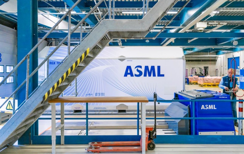
ASML is the largest supplier of Photolithography systems for the semiconductor industry across the globe. The company’s headquarter is located in Veldhoven, Netherlands, and it was founded in 1984. ASML was a joint venture between two Dutch companies, i.e., the chip-machine manufacturer, Advanced Semiconductor Materials International (ASMI), and the electronics giant Philips. With its founding, the company got the name ASM Lithography, and now it trades with the name ASML. ASML is the manufacturers of photolithography machines for the production of integrated circuits. Photolithography is a process of drawing complex patterns in the smallest size on silicon substrate known as a wafer using ultra-high-performance lenses.
The Foundational Story of ASML
Though the company was founded in 1984, the R&D for the company had already begun 14 years before that. The ideation and R&D for ASML and its products started back in 1970. The two tech giants, ASMI and Phillips, founded ASML in a leaky shed near the Philips office in Eindhoven, Netherlands. ASML’s first product was the PAS 2000 stepper, launched in 1984. The success of its first product made ASML hire more than 100 employees within one year of its founding. It also moved to a new office in Veldhoven, the same place it has its headquarter located, in 1985.
In 1986, the company came up with another new product, PAS 2500, boasting the new alignment technology, the basis for many future innovations. By 1988, the company had started to work in foreign countries, having its first joint-venture foundry established in Taiwan. The company also began to expand in the USA, starting its first five offices in various locations, with more than 80 employees. Despite the expansion, the company was unable to make a mark in the rapidly growing competition and had to ask for financial help from Philips’ board member Henk Bodt.
Since ASML was continuously working on its R&D, the raised money was used well, and the company brought its pathbreaking product, the PAS 5500, in the early 90s. The launch of PAS 5500 provided ASML all the attention, and the biggest investors wanted to support the company financially. In 1995, ASML had its first IPO and went public on the Amsterdam and New York stock exchanges. With the IPO, Philips sold most of its shares in the company and slowly parted its way from ASML in the later years.
In 2001, ASML released its another revolutionary product, the TWINSCAN system, followed by the launch of TWINSCAN AT:1150i (first immersion machine) in 2003 and TWINSCAN XT:1700i (first volume production machine for immersion) in 2006. All these innovative launches by ASML helped the companies to reduce the size of the chip to an even smaller size. ASML then acquired the semiconductor and optimization solution manufacturing company BRION, such that now ASML independently could optimize the chip manufacturing process and apply real-time measurements and corrections to the chip.
In 2010, ASML introduced its first prototype Extreme Ultraviolet (EUV) lithography tool, which could help to manufacture smaller but more powerful chips by making smaller chip features using the shorter wavelength light. To get better at EUV manufacturing and speed up the production, ASML then acquired the San Diego-based lithography light sources manufacturer, Cymer, in 2013. The company brought the NXE:3300 (second generation EUV) in the next year, and the NXE:3350 (third-generation EUV) came in 2015.
To solely rule the world of Photolithography systems, ASML then acquired the leading e-beam metrology tools supplier, Hermes Microvision (HMI), in 2016. In 2017, with this acquisition, ASML came up with the e-beam pattern fidelity metrology system (ePfm5). According to 2019 data, ASML has registered more than 12000 patents to its name.
The CEO

Peter Wennink is the President and Chief Executive Officer (CEO) of ASML. He has been working with ASML since the year 1999. He started as the Executive Vice President and was appointed the CEO of the company in 2013. He is also a member of the Board of Management at ASML. Before ASML, Wennink has also worked with companies like Deloitte Accountants.

Yashica is a Software Engineer turned Content Writer, who loves to write on social causes and expertise in writing technical stuff. She loves to watch movies and explore new places. She believes that you need to live once before you die. So experimenting with her life and career choices, she is trying to live her life to the fullest.